Abstract
The article gives a brief description of the design, fabrication, and implementation of wearable flexible sensors developed with a laser cutting technique. The approach used standardized protocols on the raw materials processed for the development of the prototypes. Four distinct types of sensor prototypes were prepared with different organic polymers as substrates and allotropes of carbon and aluminum as electrodes. The processed materials were selected based on the targeted application. These sensor patches were used for monitoring limb movements and respiration, tactile sensing, and urinary incontinence detection.
Introduction
The intervention of sensors [1] in different applications has led to a significant change in human quality of life. This in turn has triggered an increase in the demand for sensors with better performance in terms of cost, durability, and sensitivity. The materials used for developing a sensor largely depend on its application. For example, a sensor attached to a person to detect a fall would require electrodes and substrates to be developed with materials having the highest possible conductivity and flexibility, whereas for monitoring a heartbeat, a much smaller device with greater sensitivity would be needed. Therefore, the fabrication of a sensor is the most important step in determining its application. Approximately three decades ago, when sensors were first introduced, silicon sensors were most commonly developed and used because of their unique advantages, including compactness, ease of implementation, and particular electrical properties. This led to the use of the sensors in different heterogeneous applications such as gas sensing [2], [3] and determining the various constitutional elements of food products like beverages [4], [5] and meat [6]. Even though silicon sensors came to be a popular choice, they possessed certain disadvantages, which led researchers to search for better options. Flexible sensors were developed to replace the existing rigid ones, with electrodes and substrates prepared using malleable materials. A high tolerance for strain, lower fabrication costs, and great bendability are some of the advantages these sensors offer over those made of silicon. Polymeric materials often used in developing the substrates for flexible sensors include polydimethylsiloxane (PDMS) [7], polyethylene terephthalate (PET) [8], and polyimide (PI) [9].
The main differences between these polymers relate to their mass density and flexibility. The reasons behind the use of each of these materials are explained in the following section. Conductive materials commonly used with the electrodes of flexible sensors include silver [10], carbon [11], and aluminum [12]. One of the biggest advantages of using flexible sensors is that, as wearable devices, they can be used for unobtrusive tracking. The sensors along with the embedded system are attached to the body or to clothing in order to study a particular trait. In this way, the person under observation can be discreetly monitored without any discomfort or hampering of privacy. Researchers have emphasized that monitoring physiological parameters [13], [14] and body movements [15], [16] in particular could not be done with silicon sensors due to their rigidness. Various fabrication techniques are used to process the raw materials for developing the flexible sensor prototypes. Some of the more common ones are photolithography [17], screen printing [18], and laser cutting [19]. Among these, laser cutting is the easiest and quickest method for several reasons—namely, ease of sample preparation, the ability to create smooth edges, and the lack of need for experts. This article briefly describes some of the flexible sensors developed with the laser cutting technique using standardized protocols. Laser cutting has been an established technique for curving flexible sensors for some time [20], [21]. Different kinds of laser cutting machines varying in their output power are available. Those most commonly used for fabrication purposes are CO2 laser engravers [22], [23]. Design software is configured along with the laser system, with the dimensions of the prototype assigned manually. This design is transferred to the laser engraving stage to replicate these dimensions on the sample.
Fabrication of the Sensor Prototypes
The entire fabrication process was carried out inside a cleanroom with fixed temperature and humidity levels [24]. The classification level 209E, defined by federal standards, is followed by cleanrooms worldwide [25]. These standards have laid down rules regarding the amount of molecular contamination in the air per volume present in different ISO classes. The fabrication of these sensor prototypes was carried out in ISO class 6 [26], [27].
Each step in the fabrication of the sensor prototypes was taken for particular reasons. The first sensor patch was developed by forming a nanocomposite between PDMS and multi-walled carbon nanotubes (MWCNTs) [15]. The reasons for using PDMS as the substrate material for the sensor were its low cost and quicker production time [28]. Laser cutting of PDMS has been done by researchers a considerable number of times, especially in developing microfluidic channels [29]–[31]. CNTs were considered over other nanoparticles because of their light weight, high electrical conductivity, and mechanical stability. High purity, higher electrical conductivity, and less chance of defects are some of the reasons why MWCNTs were chosen over single-walled carbon nanotubes (SWCNTs) [32]. Carboxylic group (-COOH) functionalized MWCNTs were considered as the conductive material due to their high oxidative and metallic properties [33], [34]. CNTs by wt. % considered for dispersion in PDMS were determined from [35], where a range of 1 wt. % to 4.5 wt. % was taken to develop the composite electrodes. After an optimization was done on the sample, between the conductivity of the nanocomposite and the dispersion of MWCNTs into PDMS, 4 wt. % was fixed to form the electrodes. Fig. 1 shows an SEM image of the nanocomposite formed with 4 wt. % of MWCNTs in PDMS. The black and white areas in the image represent the CNTs and PDMS, respectively. Fig. 2 shows the different steps followed during the fabrication process.
![Fig. 1. SEM image of the developed CNT-PDMS nanocomposite [15].](https://www.standardsuniversity.org/wp-content/uploads/fig1-cnt-pdms.jpg)
Fig. 1. SEM image of the developed CNT-PDMS nanocomposite [15].
![Fig. 2. Individual steps followed during the fabrication of the CNT-PDMS-based flexible sensor [15].](https://www.standardsuniversity.org/wp-content/uploads/fig2-cnt-pdms.jpg)
Fig. 2. Individual steps followed during the fabrication of the CNT-PDMS-based flexible sensor [15].
The CO2 laser machines used for designing the electrodes followed a standardized ISO 115616-2:2003 [36]. This standard determines the accuracy, precision of measurement, repeatability, and trajectory. Universal Laser Systems [37] were used to perform the laser cutting for designing the electrodes. Similar to that for cleanrooms, this standardized protocol also separated the laser cutters into different classes [38]. These classes differ in terms of identified risks, hazards, and safety. These systems complied to and operated with a Class 4 laser system [39], [40]. Power, speed, and z-axis were the three parameters of the laser system that were optimized during the procedure.
While power (W) referred to the amount of energy of the laser on the sample, speed (m/min) determined how rapidly the laser nozzle would move over the processed sample. The z-axis (mm) determined the height of the platform of the system in order to adjust the focal point of the laser nozzle on the sample. Based on the cuts obtained on PDMS in [30], adjustments were made to both power and speed. Table 1 gives the different combinations tried during the process of optimizing power and speed settings.
Table 1. Different Power and Speed Combinations Tried During the Experimental Process [15].
| Power (W) | Speed (m/min) | z-Axis (mm) | Thickness of the electrodes (microns) |
| 1.2 | 4.2 | 2 | 137 |
| 2.4 | 7 | 2 | 140 |
| 12 | 42 | 2 | 150 |
| 24 | 70 | 2 | 175 |
| 42 | 126 | 2 | 180 |
![Fig. 3. Front and rear views showing the dimensions of the sensor patch [15].](https://www.standardsuniversity.org/wp-content/uploads/fig3-sensor-patch.jpg)
Fig. 3. Front and rear views showing the dimensions of the sensor patch [15].
A series of short-circuit tests proved a power of 24W and speed of 70 m/min to be the most viable setting. Fig. 3 shows the front and rear views of the sensor along with its final dimensions. A pair of the three electrodes was formed with a thickness of 200 microns and an interdigital distance of 100 microns.
The second sensor prototype was developed with metallized PET films [41]. One side of the PET film was covered with aluminum (Al). Due to the use of a single raw material, the structure of this sensor is different from other sensors. High flexibility, smooth cut edges, and the absence of any post-processing steps are some of its advantages, due to which PET was chosen as the substrate material [42], [43]. Al nanoparticles also have certain advantages that make it a viable option for the electrode material [44]. Some PET films possess high corrosion resistance, high electrical and thermal conductivity, and flexibility [45]. A schematic diagram of the fabrication steps is given in Fig. 4 [41].
![Fig. 4. Schematic diagram of the individual steps followed to develop the flexible sensors with metallized PET films [41].](https://www.standardsuniversity.org/wp-content/uploads/fig4-pet-films.jpg)
Fig. 4. Schematic diagram of the individual steps followed to develop the flexible sensors with metallized PET films [41].
![Fig. 5. Thickness of the electrode line obtained after optimization of laser parameters [41].](https://www.standardsuniversity.org/wp-content/uploads/fig5-electrode-line.png)
Fig. 5. Thickness of the electrode line obtained after optimization of laser parameters [41].
![Fig. 6. Front and rear view of the sensor patch. The front is noticeably shinier than the back due to the presence of aluminum as the electrodes [41].](https://www.standardsuniversity.org/wp-content/uploads/fig6-sensor-patch.jpg)
Fig. 6. Front and rear view of the sensor patch. The front is noticeably shinier than the back due to the presence of aluminum as the electrodes [41].
The optimized values were power: 12.6 W, speed: 70 m/min, and z-axis: 1.2 mm. Fig. 6 shows the front and rear view images of the finished product [41]. The total sensing area of the patch was 44 mm2 with a thickness of 500 microns and 300 microns of the substrate and electrodes, respectively. A pair of 12 electrodes was formed with each one having a length and width of 1.2 mm and 41 µm, respectively. The interdigital distance was 150 microns.
The third type of sensor prototype developed by laser cutting was based on photothermal induction of the polymer films to form graphene [46]. This led to an idea to develop a sensor patch using the induced conductive material to form the electrodes. The advantages of this sensor prototype are its low cost and its highly conductive material. The conductivity of the electrodes of these graphene sensors was higher than those developed with CNT-PDMS and PET-Al. Commercial PI films were used as the raw material for processing. In addition to having smooth and precision cuts up to the micron range and very high flexibility [47], another substantial benefit of using PI is its excellent thermal properties, which would be advantageous while processing it with CO2 lasers [48], [49]. The schematic diagram of the fabrication steps of the graphene sensor prototypes is given in Fig. 7. Commercial PI film [7(1)] was attached to the glass substrate in order to have a smooth surface before laser induction. The laser cutting was done on the attached films [7(2)] to form powdered graphene. The shape of the induced powder was as designed in the laser system. The optimized values of the laser parameters used during this process were power: 9 W, speed: 70 m/min, and z-axis: 1 mm. The sp3 hybridized carbon atoms in the PI films were photothermally induced to form sp2 hybridized atoms in the graphene.
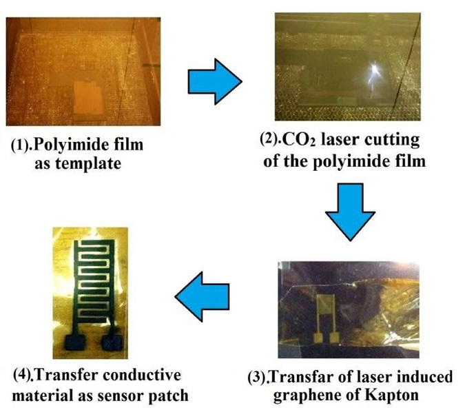
Fig. 7. Fabrication steps followed to form the graphene sensor prototypes from commercial PI films.
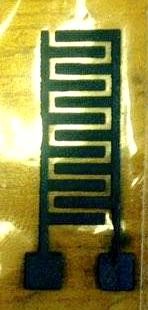
Fig. 8. Final sensor prototype.
The graphene powder was then transferred to Kapton tapes via manual stress [7(3)] for using the powdered material as the electrodes [7(4)]. The final prototype is shown in Fig. 8. The sensor patch had a pair of 6 electrodes with a sensing area of 102 mm2. The length and width of the electrode were 5 mm to 1 mm, respectively, with a distance of 500 microns between consecutive electrodes. One of the issues was the change in properties of the induced graphene during its transfer. Thus, the manual pressure exerted on the Kapton tapes during the transfer had to be done carefully as a minute of discontinuity in the transferred form would have made the sensor invalid. The change in resistivity was > 50 Ω between the formed and transferred material. Figs. 9(a) and 9(b) give the SEM images of the top view of the sensor showing the transported material on the Kapton tapes. It can be seen that the edges of the sensor prototype are relatively smooth and perpendicular to the surface.
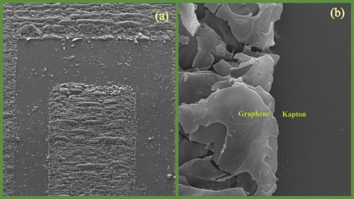
Fig. 9. SEM images of the transferred graphene on Kapton tapes.
Working Principle of the Sensor
All the sensor prototypes designed and fabricated were based on the principle of capacitive sensing. The electrodes were interdigitated with a fixed interdigital distance between two consecutive electrodes. The working principle of the sensor prototypes is shown in Fig. 10 [50]. The parallel plated electrodes were made co-planar to obtain a non-invasive single-sided measurement. The electrodes were designated as either an excitation or sensing electrode. An electric field was generated between the oppositely charged electrodes when a time-dependent voltage was provided to the excitation electrode. This generated field would bulge from one electrode to another due to the planar structure of the sensor.
![Fig. 10. Working principle of the fabrication sensor prototypes [50].](https://www.standardsuniversity.org/wp-content/uploads/fig10-working-principle.jpg)
Fig. 10. Working principle of the fabrication sensor prototypes [50].
Due to the flexible nature of the sensor patches, the expansion and contraction caused by the strain applied to it would trigger a change in response [15]. Capacitance can be defined by
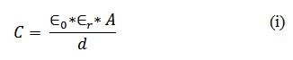
where
C is the capacitance of the material
Eo is the absolute permittivity;
Er is the relative permittivity of the material;
A is the effective area of the sensor patch;
d is the effective distance between the electrodes.
Area (A) can be divided into the length (L) and width (W) of the sensor patch. When a strain was applied to the sensor patch, this would lead to a change in the resultant area (A) and interdigital distance (d) of the patch. This would result in the change of the overall capacitance, which can be given by
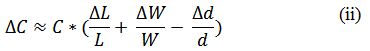
where ∆C is the change in capacitance and ∆L, ∆W, and ∆d are the changes in length, width, and interdigital distance, respectively. Fig. 11 provides a schematic of this principle.
![Fig. 11. Working principle of the sensor prototypes causing a change in its response due to the applied strain [15].](https://www.standardsuniversity.org/wp-content/uploads/fig11-working-principle.jpg)
Fig. 11. Working principle of the sensor prototypes causing a change in its response due to the applied strain [15].
Experimental Results
The fabricated prototypes were used as wearable sensing devices and utilized to monitor different physiological parameters. A HIOKI IM3536 LCR high-precision meter was used to collect the response of each sensor and store it on a computer via a USB-USB cable. The sensor was connected to the LCR meter at one end with Kelvin probes and attached at the other end using biocompatible tapes. A slow mode of testing was employed to minimize the error rate up to <0.05%. The CNT-PMDS-based sensor was used to monitor the movement of limbs by attaching the sensor to the elbow and knee of an individual. A prior profiling of the sensor with a frequency sweep between 10 kHz and 10 MHz provided an optimum frequency of 150 kHz. This frequency was fixed while performing the experiments. Figs. 12 and 13 show the changes in capacitance with the movement of the left arm and left leg, respectively [15]. “Flexed” and “extended” were the terms used to describe when the limbs were bent and kept straight, respectively. It can be seen that the flexed position causes a rise in capacitance, unlike the extended position. This occurred due to the change in the area (A) and interdigital distance (d) of the patch. The two conditions were repeated in an oscillatory motion to check the stability in the response of the sensor patch.
![Fig. 12. Response of the sensor patch regarding capacitance towards the movement of the left arm [15].](https://www.standardsuniversity.org/wp-content/uploads/fig12-sensor-patch.jpg)
Fig. 12. Response of the sensor patch regarding capacitance towards the movement of the left arm [15].
![Fig. 13. Response of the sensor patch regarding capacitance towards the movement of left leg [15].](https://www.standardsuniversity.org/wp-content/uploads/fig13-sensor-patch.jpg)
Fig. 13. Response of the sensor patch regarding capacitance towards the movement of left leg [15].
![Fig. 14. Response of the sensor patch towards the monitoring of respiration of two volunteers [15].](https://www.standardsuniversity.org/wp-content/uploads/fig14-sensor-patch.jpg)
Fig. 14. Response of the sensor patch towards the monitoring of respiration of two volunteers [15].
![Fig. 15. Response of the sensor towards tactile sensing [41].](https://www.standardsuniversity.org/wp-content/uploads/fig15-sensor-response.jpg)
Fig. 15. Response of the sensor towards tactile sensing [41].
The graphene-PI sensors were employed to test different salt concentrations in order to investigate an idea for urinary incontinence faced by the elderly. Urinary incontinence, in simple terms, can be defined as a loss of control of the urinary bladder, leading to the accidental or involuntary loss of urine. This can cause embarrassment for the person suffering from it. This problem can be triggered by high levels of stress, stones in the urinary track, multiple sclerosis, Parkinson’s disease, etc. Pregnancy, childbirth, and menopause make urinary incontinence more common among women than men. The aim would be to design a low-cost system that could be operated by nonexperts to detect urinary incontinence. Among the various elements which comprise urine, salt in the form of sodium ions is present. Therefore, experiments were conducted with different salt concentrations to assess the ability of the sensor to detect such small concentrations. A series of solutions ranging from 5 ppm to 30 ppm with a difference of 5 ppm were prepared by mixing laboratory-grade sodium chloride and de-ionized water (resistance: 18.2 MΩ). A principal solution of 100 ppm was initially prepared from the dilution solutions, which were formulated by pipetting. A frequency sweep was done between 10 Hz and 10 kHz to determine the sensitive region of the patch. The response of the sensor patch regarding phase angle vs. frequency is shown in Fig. 16. One of the frequencies was fixed from the sensitive region to develop a characteristic curve of the sensor. Fig. 17 shows the curve developed with the sensor response in terms of resistance (MΩ) vs. concentration (ppm). This frequency would be fixed in the sensor to form an embedded system in the process of developing a complete urinary incontinence detection system.
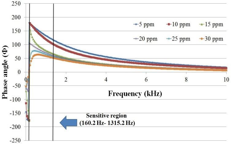
Fig. 16. Response of the graphene-PI towards different salt concentrations. The frequency-sensitive region was obtained by testing the sensor with a frequency sweep between 10 Hz and 10 kHz.
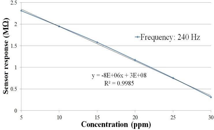
Fig. 17. Standard curve for different tested concentrations in terms of resistance.
Conclusion
The design, fabrication, and implementation of some novel wearable sensors were explained in this article. In order to develop the sensors, three different types of flexible materials were selected based on their particular properties. A laser cutting technique was employed in curving the electrodes in all three sensor prototypes. These sensor patches were utilized to monitor different physiological parameters on a primary scale. Limb movements, respiration, tactile sensing, and urinary incontinence detection were focused on as primary applications for the fabricated sensors. The next step would be to develop more wearable flexible sensors based on the ideas imparted in this article and also utilize these developed sensors to monitor other physiological parameters.
Acknowledgment
The authors would like to acknowledge King Abdullah University of Science and Technology (KAUST), Saudi Arabia, for providing research facilities for designing and developing the sensor prototypes. The authors would also like to thank Macquarie University for the opportunity to characterize and test the fabricated prototypes.
References
- M. Sze, Semiconductor sensors, New York, NY, USA: Wiley, 1994.
- A. Nag, A. I. Zia, X. Li, S. C. Mukhopadhyay, and J. Kosel, “Novel sensing approach for LPG leakage detection: Part I—Operating mechanism and preliminary results,” IEEE Sens. J., vol. 16, no. 4, pp. 996–1003, Feb. 2016.
- A. Nag, A. I. Zia, X. Li, S. C. Mukhopadhyay, and J. Kosel, “Novel sensing approach for LPG leakage detection—Part II: Effects of particle size, composition, and coating layer thickness,” IEEE Sens. J., vol. 16, no. 4, pp. 1088–1094, Feb. 2016.
- A. I. Zia et al., “Development of Electrochemical Impedance Spectroscopy based sensing system for DEHP detection,” in 2011 5th Int. Conf. Sensing Techonology (ICST), pp. 666–674.
- A. I. Zia, M. S. A. Rahman, S. C. Mukhopadhyay et al., “Technique for rapid detection of phthalates in water and beverages,” J. Food Eng., vol. 116, no. 2, pp. 515–523, 2013.
- S. C. Mukhopadhyay and C. P. Gooneratne, “A novel planar-type biosensor for noninvasive meat inspection,” IEEE Sens. J., vol. 7, no. 9, pp. 1340–1346, Sept. 2007.
- G. Comina, A. Suska, and D. Filippini, “PDMS lab-on-a-chip fabrication using 3D printed templates,” Lab Chip, vol. 14, no. 2, pp. 424–430, 2014.
- M. X. Jing, C. Han, M. Li, and X. Q. Shen, “High performance of carbon nanotubes/silver nanowires-PET hybrid flexible transparent conductive films via facile pressing-transfer technique,” Nanoscale Res. Lett., vol. 9, no. 1, pp. 1–7, Oct. 2014.
- J. H. Moon, D. H. Baek, Y. Y. Choi et al., “Wearable polyimide–PDMS electrodes for intrabody communication,” J. Micromech. Microeng., vol. 20, no. 2, p. 025032, Feb. 2010.
- D. Langley, G. Giusti, C. Mayousse et al., “Flexible transparent conductive materials based on silver nanowire networks: A review,” Nanotechnology, vol. 24, no. 45, pp. 452001, Oct. 2013.
- M. Amjadi and I. Park, “Carbon nanotubes-ecoflex nanocomposite for strain sensing with ultra-high stretchability,” in 2015 28th IEEE Int. Conf. Micro Electro Mechanical Systems (MEMS), pp. 744–747.
- S. Karki and J. Lekkala, “Film-type transducer materials PVDF and EMFi in the measurement of heart and respiration rates,” in IEEE Int. Conf. Eng. Medicine Biology Soc. (EMBS), pp. 530–533, 2008.
- Y. Jiang, H. Hamada, S. Shiono et al., “A PVDF-based flexible cardiorespiratory sensor with independently optimized sensitivity to heartbeat and respiration,” Procedia Eng., vol. 5, pp. 1466–1469, 2010.
- Y. Y. Chiu, W. Y. Lin, H. Y. Wang et al., “Development of a piezoelectric polyvinylidene fluoride (PVDF) polymer-based sensor patch for simultaneous heartbeat and respiration monitoring,” Sens. Actuators A-Phys., vol. 189, pp. 328–334, Jan. 2013.
- A. Nag, S. C. Mukhopadhyay, and J. Kosel, “Flexible carbon nanotube nanocomposite sensor for multiple physiological parameter monitoring,” Sens. Actuators A-Phys., vol. 251, pp. 148–155, Nov. 2016.
- S. Yao and Y. Zhu, “Wearable multifunctional sensors using printed stretchable conductors made of silver nanowires,” Nanoscale, vol. 6, no. 4, pp. 2345–2352, 2014.
- E. F. Nuwaysir, W. Huang, T. J. Albert et al., “Gene expression analysis using oligonucleotide arrays produced by maskless photolithography,” Genome Res., vol. 12, no. 11, pp. 1749–1755, Nov. 2002.
- W. Y. Chang, T. H. Fang, H. J. Lin, Y. T. Shen, and Y. C. Lin, “A large area flexible array sensors using screen printing technology,” J. Display Technol., vol. 5, no. 6, pp. 178–183, June 2009.
- M. Schuettler, S. Stiess, B. V. King, and G. J. Suaning, “Fabrication of implantable microelectrode arrays by laser cutting of silicone rubber and platinum foil,” J. Neural Eng., vol. 2, no. 1, pp. S121–S128, Mar. 2005.
- G. Chryssolouris, Laser machining: Theory and practice, New York, NY, USA: Springer Science & Business Media, 1991.
- J. Hillman, Y. Sukhman, D. Miller, M. Oropeza, and C. Risser, “Multiwave hybrid laser processing of micrometer scale features for flexible electronic applications,” in Proc. SPIE. 9736, Laser-based Micro- and Nanoprocessing X, p. 97360E, Mar. 2016.
- A. Kumar, N. S. Bandeshah, A. N. Nripjit et al., “State of the art of CO2 laser beam machining,” Int. J. Emerg. Technol. Adv. Eng., vol. 4, no. 4, pp. 993–999, 2014.
- “Laser engraving and cutting system.” [Online]. Accessed on Apr. 14, 2017.
- “FEDERAL STANDARD 209E FOR CLEANROOM.” [Online]. Accessed on Apr. 14, 2017.
- “FS 209E and ISO 14644 cleanroom classification standards.” [Online]. Accessed on Apr. 14, 2017.
- “FS209E and ISO cleanroom standards.” [Online]. Accessed on Apr. 14, 2017.
- “ISO cleanroom classifications.” [Online]. Accessed on Apr. 14, 2017.
- “PDMS: Fabrication and key features.” [Online]. Accessed on Apr. 14, 2017.
- Z. Isiksacan, M. T. Guler, B. Aydogdu, I. Bilican, and C. Elbuken, “Rapid fabrication of microfluidic PDMS devices from reusable PDMS molds using laser ablation,” J. Micromech. Microeng., vol. 26, no. 3, p. 035008, 2016.
- A. W. Holle, S. H. Chao, M. R. Holl, J. M. Houkal, and D. R. Meldrum, “Characterization of program controlled CO2 laser-cut PDMS channels for lab-on-a-chip applications,” in IEEE Int. Conf. Automation Science and Engineering, pp. 621–627, 2007.
- H. B. Liu and H. Q. Gong, “Templateless prototyping of polydimethylsiloxane microfluidic structures using a pulsed CO2 laser,” J. Micromech. Microeng., vol. 19, no. 3, p. 037002, 2009.
- A. Eatemadi, H. Daraee, H. Karimkhanloo et al., “Carbon nanotubes: Properties, synthesis, purification, and medical applications,” Nanoscale Res. Lett., vol. 9, no. 1, p. 393, 2014.
- N. G. Sahoo, S. Rana, J. W. Cho et al., “Polymer nanocomposites based on functionalized carbon nanotubes,” Prog. Polym. Sci.,, vol. 35, no. 7, pp. 837–867, 2010.
- C. X. Liu and J. W. Choi, “Improved dispersion of carbon nanotubes in polymers at high concentrations,” Nanomaterials, vol. 2, no. 4, pp. 329–347, 2012.
- H. C. Jung et al., “CNT/PDMS composite flexible dry electrodesfor long-term ECG monitoring,” IEEE Trans. Biomed. Eng., vol. 59, no. 5, pp. 1472–1479, May 2012.
- “ISO standards for CO2 laser cutters.” [Online]. Accessed on Apr. 14, 2017.
- “PLS user guide.” [Online]. Accessed on Apr. 14, 2017.
- “Laser cutter classes.” [Online]. Accessed on Apr. 14, 2017.
- “Universal laser systems.” [Online]. Accessed on Apr. 14, 2017.
- “Class 4 conversion module.” [Online]. Accessed on Apr. 14, 2017.
- A. Nag, S. C. Mukhopadhyay, and J. Kosel, “Tactile sensing from laser-ablated metallized PET films,” IEEE Sens. J., vol. 17, no. 1, pp. 7–13, Jan. 2016.
- “Laser cutting and engraving of PET.” [Online]. Accessed on Apr. 14, 2017.
- “Cutting PET with CO2 laser.” [Online].
- A. de la Escosura-Muñiz, M. Espinoza-Castañeda, M. Hasegawa et al., “Nanoparticles-based nanochannels assembled on a plastic flexible substrate for label-free immunosensing,” Nano Res., vol. 8, no. 4, pp. 1180–1188, Apr. 2015.
- “Aluminium: Advantages and properties of aluminium.” [Online]. Accessed on Apr. 14, 2017.
- J. Lin, Z. Peng, Y. Liu et al., “Laser-induced porous graphene films from commercial polymers,” Nat. Commun., vol. 5, 2014.
- “Laser cutting of polyimide.” [Online]. Accessed on Apr. 14, 2017.
- “Processing plastics with CO2 lasers.” [Online]. Accessed on Apr. 14, 2017.
- G. B. Collins, “Laser processing of polyimide on copper,” M.S. thesis, Dept. Elect. Eng. Virginia Polytech. Inst. and State Univ., Blacksburg, 2001.
- M. S. A. Rahman, S. C. Mukhopadhyay, and P. L. Yu, “Novel planar interdigital sensors,” in Novel Sensors for Food Inspection: Modelling, Fabrication and Experimentation. Cham, CH: Springer Int., 2014. pp. 11–35.
- R. D. P. Wong, J. D. Posner, and V. J. Santos, “Flexible microfluidic normal force sensor skin for tactile feedback,” Sens. Actuators A-Phys., vol. 179, pp. 62–69, 2012.
- J. Engel, J. Chen, and C. Liu, “Development of polyimide flexible tactile sensor skin,” J. Micromech. Microeng., vol. 13, no. 3, pp. 359–366, 2003.
- R. S. Dahiya et al., “Towards tactile sensing system on chip for robotic applications,” IEEE Sens. J., vol. 11, no. 12, pp. 3216–3226, June 2011.
- R. S. Dahiya, G. Metta, M. Valle, and G. Sandini, “Tactile sensing—from humans to humanoids,” IEEE Trans. Robot., vol. 26, no. 1, pp. 1–20, Feb. 2010.
 Mr. Anindya Nag (anindya1991@gmail.com) has completed his Bachelor of Technology degree on Electronics and Communication from West Bengal Institute of Technology, India in 2013 and received his Master of Engineering (M.E.) degree from Massey University, New Zealand in June 2015. His major during his M.E. degree was Electronics and Computer Systems. His research interests are in the area of Smart Sensors and Sensing Technology for home and environmental monitoring. He is currently pursuing Ph.D. in Faculty of Engineering at Macquarie University, Australia and is working on Printed Flexible Sensors for Human Wellness.
 Dr. Subhas Chandra Mukhopadhyay (M’97, SM’02, F’11; Subhas.Mukhopadhyay@mq.edu.au) graduated from the Department of Electrical Engineering, Jadavpur University, Calcutta, India with a Gold medal and received the Master of Electrical Engineering degree from Indian Institute of Science, Bangalore, India. He has Ph.D. (Eng.) degree from Jadavpur University, India and Doctor of Engineering degree from Kanazawa University, Japan. Currently he is working as a Professor of Mechanical/Electronics Engineering with the Department of Engineering, Macquarie University, New South Wales, Australia. He is the Program Leader of the Mechatronics Engineering Degree Program. He has over 26 years of teaching and research experiences. His fields of interest include Smart Sensors and Sensing Technology, Wireless Sensor Networks, Instrumentation and Measurements, Internet of Things, Environmental Measurements, Electromagnetics, Control Engineering, Mechatronics, Magnetic Bearing, Fault Current Limiter, Electrical Machines and numerical field calculation etc. He has authored/co-authored over 400 papers in different international journals, conferences and book chapter. He has edited fifteen conference proceedings. He has also edited seventeen special issues of international journals as lead guest editor and thirty books with Springer-Verlag. He was awarded numerous awards throughout his career and attracted over US$3.0 M on different research projects. He has delivered 296 seminars including keynote, tutorial, invited and special seminars. He is a Fellow of IEEE (USA), a Fellow of IET (UK) and a Fellow of IETE (India). He is a Topical Editor of IEEE Sensors Journal, and an Associate Editor IEEE Transactions on Instrumentation and Measurements. He is in the editorial board of e-Journal on Non-Destructive Testing, Sensors and Transducers, Transactions on Systems, Signals and Devices (TSSD). He is the co-Editor-in-chief of the International Journal on Smart Sensing and Intelligent Systems. He was the Technical Program Chair of ICARA 2004, ICARA 2006, ICARA 2009 and IEEE I2MTC 2016. He was the General chair/co-chair of ICST 2005, ICST 2007, IEEE ROSE 2007, IEEE EPSA 2008, ICST 2008, IEEE Sensors 2008, ICST 2010, IEEE Sensors 2010, ICST 2011, ICST 2012, ICST 2013, ICST 2014, ICST 2015 and ICST 2016. He has organized the IEEE Sensors conference 2009 at Christchurch, New Zealand during October 25 to 28, 2009 as the General Chair. He is currently organizing the 11th ICST in Sydney, Australia during December 4-6, 2017. He is the Ex-Chair of the IEEE Instrumentation and Measurement Society New Zealand Chapter. He is a Distinguished Lecturer of IEEE Sensors Council from 2017-2019.